Periodically there maybe a need to verify via inspection that the footprint on
the bare PC board assembly for a component matches the footprint (correct
solder pad size and land pattern)
for the same component listed in the
Bill of Materials (BOM).
The mismatch of component footprint spacing is usually an error created
when
components on the PCB assembly ( PCBA ) are part sourced and then those part sourced components
are reflected in the BOM that is then used to assemble the PCB. The problem occurs when the components that are part sourced are incorrectly
chosen and do not match the footprint spacing initially specified when the PCBA was originally designed on the CAD system.
Also the
mismatch of component footprint spacing may occur when the
wrong components are purchased that do not match those listed in
the BOM or an error during kitting. In these cases these components during
assembly may not fit the landing pad area on the bare PC board.
There are several methods using the Unisoft software for crosschecking
the component footprint in the CAD file or bareboard gerbers with the shapes
listed via the part numbers in the BOM and below are listed some of those
options. The procedures listed below assume some
working knowledge of the Unisoft software. Please contact Unisoft
directly for details.
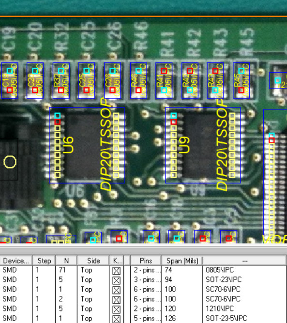
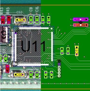
Note that for all shape crosschecking methods listed below on this webpage
visual details of many types can be added to the display as desired. For
example as in the figure below a photograph of the bare or loaded PCB assembly ( PCBA ) board can
be added to the display and the part shape information, manufacturers part
number and other information from the Bill of Material (BOM) can be overlaid on
the components and this can be compared the the component pins display from the
CAD file imported into the Unisoft software. At that point
mismatch of component footprints can be detected.
Further Gerber silkscreen information, etc. can be overlayed on the display.
Additionally each part number and its components can be blinked on the display
and also checked off and colored for inspection verification.
Also user hyperlinks to any component information (footprint, electrical, ECO,
etc.) can be added for each part number or use the direct links supplied in the
Unisoft software to the manufacturer part number information available from
popular part source vendor such as Digikey, Ultra Librarian, Sourcengine,
Octopart, FindChips, etc.
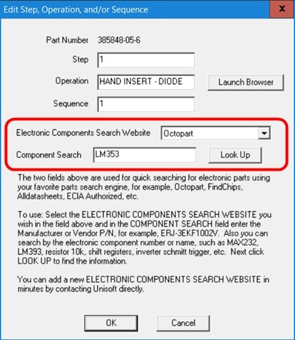
IMPORT THE
CAD OR GERBER FILE AND BOM AND CHECK THE FOOTPRINT DIMENSIONS THE BOM PART
NUMBER INDICATES:
For aiding inspection in checking the component footprint on the PCB assembly ( PCBA ) for the correct solder pad size and land pattern to the component listed in the Bill of Material (BOM) the Unisoft software allows you to import either the CAD or Gerber files or both. Then you can import the BOM data and that information is now displayed and associated with the components on the PCB.
There can be as many Library files as desired, and this example Library file above can contain an unlimited amount of part numbers. The part numbers listed above, such as 381200-40-1, 381200-66-4, etc. in the example library above are in-house and not standardized part numbers. Where possible it's best to have a part number that's linked to a standard such as the Manufacturer's Part Number (MPN), for example these are MPN part numbers CC0402CRNPO9BN2R2, RC0201JR-0710RL, DS520-30EAA02 and MPN part numbers are standard and common to everyone around the world.
So the next step is to import the library by clicking the FILE menu then
click IMPORT LIBRARY and the result would be similar to the picture below.
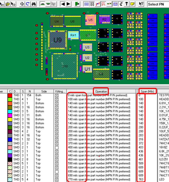
In the picture below the library items indicating the span that represent
the BOM are now under the Operation fields on the left outlined in red and
the actual component span data measured from the CAD data for the PC board
is on the right outlined in red. So the PC Board inspector can do a
quick look between those two columns and the numbers should match or be
close and this would indicate that the component packages in the BOM and the
footprint on the PC Board are the same or within a reasonable size range of
each other.
In this method we will be checking for:
- The span of components on the PCB assembly ( PCBA ) against the BOM
using the Smart Color window on the display.
- A crosscheck done by comparing the device pin count
on the PCB assembly ( PCBA ) board layout to the BOM using the Smart
Color window on the display. .
SPAN CROSSCHECK:
The Unisoft software imports the CAD or Gerber files and then calculates the
maximum span of all components on the PC board. This span measurement is the
furthest distance of the centers of any 2 pins on the device. So for
example for a 2 pin device 0603 package the span distance would be measured and
listed as approximately 60 mils. This can then be compared to what is listed for
the same device and the BOM when it is imported into the Unisoft software and if
there is a discrepancy it can be addressed.
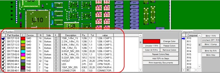
For example using the Unisoft Smart Color window on the display quality inspection of the components can be validated from the foot print of
the component on the board to what is listed in the BOM.
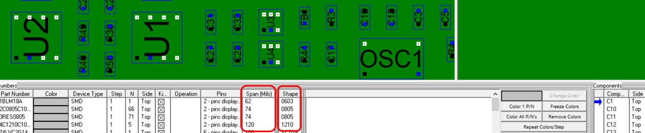
The Smart Color window in the Unisoft software is displayed in the figure below
and in one of the columns is the Shape footprint indicated in the BOM and the
other column is the Span (Mils) and this field is the actual measured
distance of the component on the PC board. These 2 columns should correlate
and if they do not then there is a discrepancy that should be investigated.
Note that above the span measurement is from the centers of the 2 extreme pins on the
device. So for example a 0603 device listed in the BOM would be thought to be 60
mils but the actual measurement calculated maybe slightly more or less and still
be correct.
For example in the figure above it is 62 mils for one of the 0603 shape
component part numbers. And 74 mils for the two 0805
shape component part numbers (0805 would be approximately 80 mils). Then
for the 1210 shape component part number the span measured is 120 mils (a 1210
shape would be approximately 120 mils).
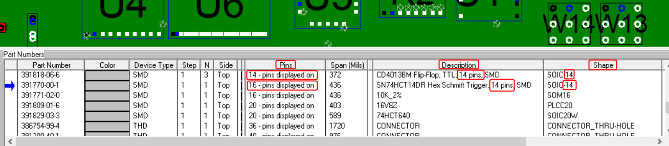
PIN COUNT CROSSCHECK:
Also a crosscheck can be done by comparing the device pin count on the PCB assembly ( PCBA ) board
layout to the BOM and this is done by using the Pins field
located in the
Smart Color window.
In the
figure below we
see that the Pins field gives the total number of
pins for each part number and this field can be used to verify against the
BOM. For example if the Pins field which represents the PCB assembly ( PCBA ) layout
indicates that there are 16 pins for that device part number and in the BOM it
indicates that there are 14 pins then an error has been detected. In the
figure below both the Description and the Shape fields where imported from the
BOM and either field may indicate a
discrepancy
in the board footprint to BOM footprint crosscheck.
The first part number in the figure below indicates that it is both 14 pins in
the Pins field and also in the Description field it is 14 pins and further in
the Shape field it is an SOIC-14 which is 14 pins and so this part number does
not have a pins count
discrepancy.
However in the second part number below we see that the Pins field indicates
that it's 16 pins on the PCB assembly ( PCBA ) however both the Description field and the
Shape field from the BOM indicates that it's 14 pins so we know there's a
discrepancy
in our board
footprint to BOM footprint crosscheck.
In this method we will be checking for the span of components on the PCB assembly ( PCBA ) against the BOM
using a file created.
The Unisoft software imports the CAD or Gerber files and then calculates the
maximum span of all components on the PC board. This span measurement is the
furthest distance of the centers of any 2 pins on the device. So for
example for a 2 pin device 0603 package the span distance would be measured and
listed as approximately 60 mils. This can then be compared to what is listed for
the same device and the BOM when it is imported into the Unisoft software and if
there is a discrepancy it can be addressed.
For example using the Output Flat File feature of the software a file can be
exported and then quality inspection of the components can be validated from the foot print of
the component on the board to what is listed in the BOM.
We have used the Output Flat File feature of the software to create the file in
the figure below and in one of the columns is the Shape footprint indicated in
the BOM and the other column is the Span (Mils) and is the actual measured
distance of the component on the PC board. These 2 columns should correlate
and if they do not then there is a discrepancy that should be investigated.
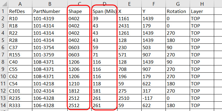
Note that the span measurement is from the centers of the 2 extreme pins on the device. So for example a 0603 device listed in the BOM would be thought to be 60 mils but the actual measurement calculated maybe slightly more or less. For example in the figure above it is 71 mils for one of the 0603 shape components and 59 mils for the other 0603 component.
IMPORT THE
CAD OR GERBER FILE AND BOM AND CHECK THE FOOTPRINT DIMENSIONS:
For aiding inspection in checking the component footprint on the PCB assembly ( PCBA ) for the correct solder pad size and land pattern to the component listed in the Bill of Material (BOM) the Unisoft software allows you to import either the CAD or Gerber files or both. Then you can import the BOM data and that information is now displayed and associated with the components on the PCB.
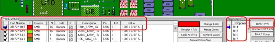
You can then blink by part number and those components will blink on the display. Even if there are multiple components for the part number usually only 1 component in each part number on the Unisoft display needs to be inspected to make sure the component spacing on the PCB assembly ( PCBA ) bare board fits what's listed in the BOM.
For example if the part number in the BOM indicates a 1206 component shape then
the footprint on the PCB assembly ( PCBA ) bare board where the components for the selected part
number are blinking
should have that shape also (correct
solder pad size and land pattern). So in the figure below usually only 1
component, such as R14 or R15, needs to be inspected of the 16 component
reference designators listed for that part number.
You can also have dimension data displayed to aid the inspection.
Dimension data can be displayed in the OPERATION window and then the Measurement
Tool can be used to measure the footprint for the component on the PCB assembly ( PCBA ) and if
they match then the crosscheck is good.
For example in the picture below we are checking only one reference designator
R10 for the part number 391727-10-9 . We located R10 by blinking it on the
display which from the OPERATION field indicates it is 3.22mm and if
that is what's measured then the crosscheck is ok and we can move onto the next
part number.
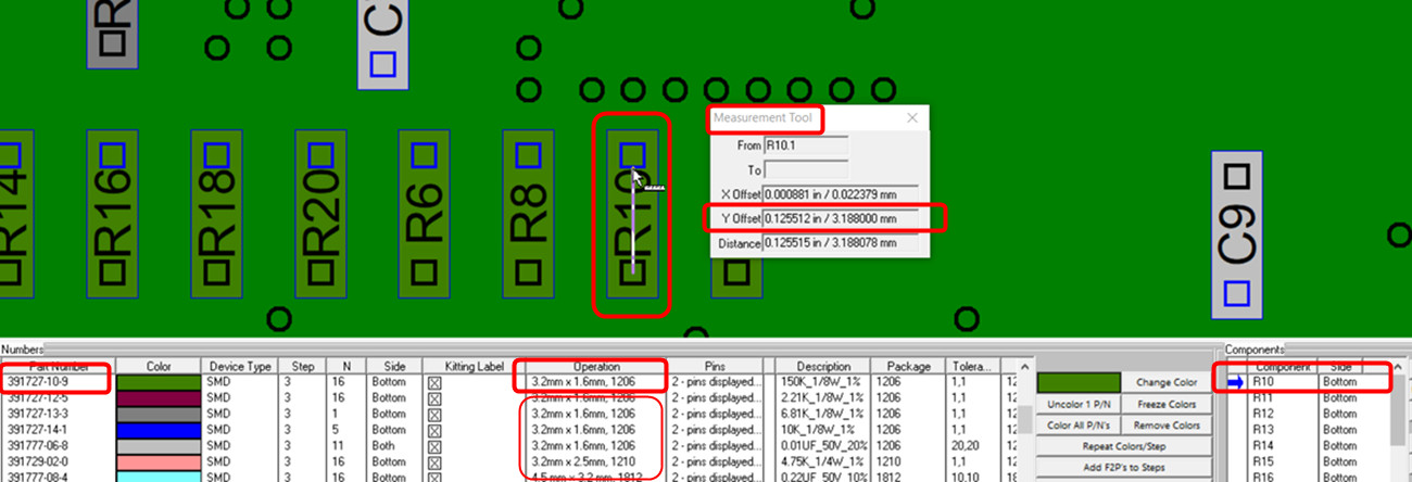
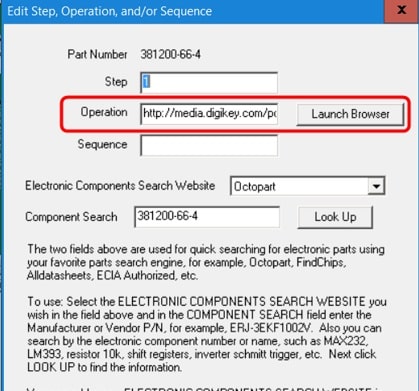
The OPERATION field can be populated 3 ways. Either automatically from the BOM or manually from the Smart Color window or it can be populated from a library similar to the one below .
390222-06-2 0.25mm x 0.125mm, 0201
390222-07-1 0.4 mm × 0.2 mm, 0402
390579-03-3 2.0mm x 2.0mm, SOT23
391729-02-0 3.2mm x 2.5mm, 1210
391727-10-9 3.2mm x 1.6mm, 1206
391727-12-5 3.2mm x 1.6mm, 1206
391727-13-3 3.2mm x 1.6mm, 1206
391727-14-1 3.2mm x 1.6mm, 1206
391777-06-8 3.2mm x 1.6mm, 1206
391777-08-4 4.5 mm × 3.2 mm, 1812
395422-01-9 4.8mm x 3.8mm, SOIC8
391818-06-6 7.62mm x 5.75mm, SOIC14
391809-01-6 8.8mm x 8.8mm, PLCC20
391829-03-3 10.3mm x 2.25mm, SOIC20
391770-01-2 11.2mm x 5.6mm, SOM16
391770-02-0 11.2mm x 5.6mm, SOM16
395391-01-6 15.5mm x 15.5mm, PLCC20 Socket
391822-01-2 15.88mm x 7.49mm, SOIC48
391822-02-0 15.88mm x 7.49mm, SOIC48
391822-03-9 15.88mm x 7.49mm, SOIC48
390607-01-0 16.510mm x 16.510mm, PLCC44
390579-03-3 25.019mm x 25.019mm, PLCC68
Many manufacturers of semiconductor IC's and passive components use package
outlines and dimensions according to JEDEC, IEC and JEITA
organization
standards but there can be products also in non-standard package outlines.
OPTIONAL:
BRING IN A PHOTO OF THE BARE OR LOADED PCB.
To add more realism to the display for solder pad size, land pattern, etc. you can also bring in a photo of the bare or loaded PC Board and place it to the back of the display to enhance the visual detail of the components being blinked and inspected.
OPTIONAL:
LOOKUP THE COMPONENT SHAPE, ETC, INFORMATION VIA DIGIKEY, OCTOPART,
FINDCHIPS, ETC.
You can lookup the component shape information and more via Digikey, Octopart,
Findchips, etc. Components can be
searched by vendor part number or electronic component number or name.
The result is component information such as part footprint shape, electrical specifications, cost, availability, etc. is displayed.
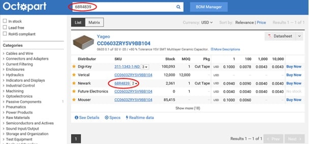
The component footprint dimensions (correct solder pad size and land pattern) can be found.
Also the internal electronic functionality, etc. can be searched.
OPTIONAL: AUTOMATICALLY LOAD THE SHAPE INFORMATION VIA THE UNISOFT LIBRARY INTO THE OPERATION ASSOCIATED WITH THE PART NUMBER.
A simple library associating the component part number with any component information you wish via a link on the web or on your server can be created. For example the link can point to component shape information for crosschecking the footprint in the cad file or bareboard gerbers with the shapes listed in the part numbers in the BOM.
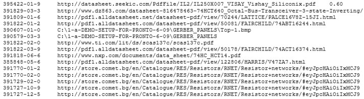
Those links can be imported automatically and match to the part number on the display.
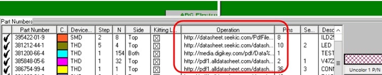
The browser can then be launched and the result is any type of component information you have at that link is displayed. For example detailed inspection information such as footprint shape pad size, electrical specifications, cost, availability, etc.
For example the component footprint dimensions (correct solder pad size and land pattern).
MISC: CHECKING GERBER DATA TO THE BARE BOARD VIA PHOTO.
On occasion there may be a need to check the bare board to the Gerber data for footprint lineup, etc. In this case we are not concerned about any BOM issues.
To do this bring the Gerber data into the Unisoft software then optionally Make the components. Bring in a photograph of the bare PC Board using the annotation tool and send it to the back of the display. At this point the bare PC Board pads from the photo can be checked that they line up with the Gerber footprints displayed.
MISC: CHECKING CAD DATA TO THE BARE BOARD GERBER DATA OR PHOTO OF THE BARE BOARD.
On occasion there may be a need to check the bare board to the CAD data for footprint lineup, etc. In this case we are not concerned about any BOM issues.
To do this bring the CAD data into the Unisoft software then either use the Ad Layer feature to add Gerber on top of the CAD data or bring in a photograph of the bare PC Board using the annotation tool and send it to the back of the display. At this point the bare PC Board pads from either the Gerber data or photo can be checked that they line up with the CAD data footprints displayed.