Skip navigation
For over 40 years, Intelligent PCB Manufacturing
Automation Software
Be production ready in minutes, not days.

Below is the Unisoft Free Distance Calculator for
components on the PCB. Using this calculator, you can identify component
pins on unique reference designators where the pins on the components are
equal to or less than the distance you specify, for example, 75 mils (0.075
inches).
This calculator can be used, for instance, to detect
components that may be too close together, potentially causing quality
issues.
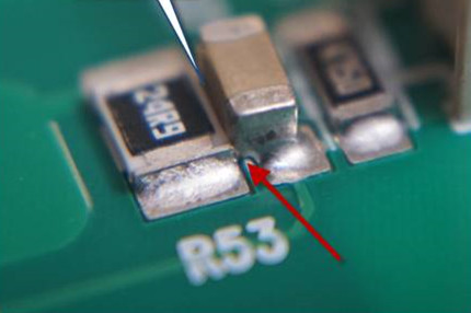
It is also useful for identifying SMT components that might
impact the design and effectiveness of a wave solder pallet. Typically,
there may be space to reposition the SMT components away from the thru-hole
solder joint, but during the PCB design phase, designers may be unaware that
such adjustments are necessary. Wave solder pallets are a special type
of fixture used during the wave soldering process to mask selected areas of
the printed circuit boards that require thermal or solder protection, for
example thru-hole devices. The
masked areas usually contain SMT components, ground planes, gold fingers
and/or mounting holes.
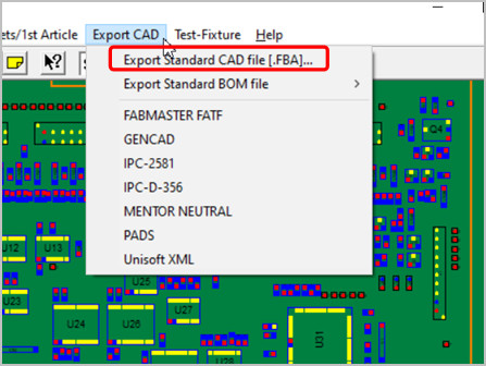
Export a .FBA File:
.FBA file. To
export the .FBA file, click EXPORT CAD, then click EXPORT STANDARD
CAD FILE [.FBA], and save the file to the directory of your choice. 
The Calculator:
.FBA file to
compare each pin against all others on the PCB.
Running The Calculator: In the first box below,
click the 'BROWSE / CHOOSE FILE' button. Browse to the
.FBA file you wish to import, select the file, and then click
'OPEN'.
Enter the distance in the second box you
wish to check, in inches. Note: If a large number is entered, the resulting
list can become very large. It is recommended to use a reasonably smaller
number, typically under 0.20 inches.
Process the File by clicking
the 'PROCESS FILE' button. Any relevant data will be displayed below.
The tool calculates the distance between closely spaced pins up to
the specified limit. For example, it identifies all pins on unique reference
designators that are 150 mils (0.150 inches) apart or less, as shown in the
sample format below:
Ref. Des. #1 Pin
X Y
Surface Ref.
Des. #2 Pin X
Y Surface
Distance Between Pins
U4
11 -5.475 2.240
T
U6
48 -5.388 2.240
T
0.0870
R41
1 -5.250
1.395 T
U9
35 -5.350 1.400
T
0.1001
C1
1 -4.800
0.320 T
U1
14 4.700
0.360 T
0.1077
If you wish to save the data, the default file name is
'outputData.txt', displayed in the box below. You may change the file name
if desired. Once ready, click the 'SAVE DATA TO FILE' button to save the
data.
The above calculator is provided for informational purposes only.
Unisoft assumes no responsibility for any issues that may arise from its
usage.
Design for Manufacturing/Assembly/Test (DFM/DFA/DFT) for PCB
Manufacturing
Design for Manufacturing, Assembly, and Test
(DFM/DFA/DFT) for PCB manufacturing is a broad and complex subject area.
This comprehensive approach is aimed at designing printed circuit boards
(PCBs) in a manner that facilitates easier and more cost-effective
manufacturing.
DFM/DFA/DFT checks focus on optimizing the PCB design to align with manufacturing capabilities while minimizing potential issues that could arise during production. The primary goals are to enhance production efficiency, reduce costs, and ensure the quality of the final product.
Most aspects of DFM/DFA/DFT are addressed during the PCB design phase, utilizing sophisticated software and techniques provided by various CAD systems. These systems are essential for PCB design, with hundreds of DFM/DFA/DFT criteria to be verified. When applied correctly, adequate DFM/DFA/DFT measures ensure that potential manufacturing, assembly, and testing issues are mitigated before production begins.
Unisoft software, which imports various CAD files and Bills of Materials (BOM) from PCB CAD design systems, assists in verifying that DFM/DFA/DFT principles have been effectively applied to certain aspects of PCB design. For more detailed information on these methods, contact Unisoft directly or refer to the online help tooltips provided.
Areas where
the Unisoft software may assist in verifying that DFM / DFA / DFT was executed properly:
Component Placement
Spacing: The Unisoft software cross-checks that proper spacing between
components is maintained on the PCB by measuring the distance between pins
for unique
reference designators. This spacing is
typically addressed during the design phase of the PCB. Proper component
spacing enables efficient assembly and minimizes issues during soldering
processes.
Test Probe Access
Nets: The Unisoft software verifies that proper test probe access is
available by analyzing each electrical net trace to ensure accessibility for
test probes. This is also typically
addressed during
the PCB design phase. Ensuring adequate test probe access minimizes issues
during the testing phase of manufacturing, including functionality and
quality assurance. This
is a critical Design for Test
(DFT) consideration that facilitates In-Circuit Testing (ICT), Flying Probe
Testing, Functional Testing, and more.
PCB Test Probe Force
Analysis Visualization: Analyzes stresses on the PCB induced by
test probes that press into the PCB, with consideration for offset vectoring
via the placement of push fingers.
Assembly and
Fabrication Notes: Includes detailed notes and specifications for the
manufacturer regarding assembly processes, material requirements, and any
special handling or processing
needs. The Unisoft
software creates process assembly documents to facilitate this.
Supply Chain Considerations:
Design for Manufacturing (DFM), Design for Assembly (DFA), and Design for
Testability (DFT) can extend to include considerations of the supply chain,
such as the
availability of components, lead times,
and the impact of using alternate parts. Early consideration of these
factors helps avoid delays and redesigns caused by unavailable parts or
longer-than-expected
lead times. The Unisoft
software's lookup feature by manufacturer part number, among other
capabilities, can significantly aid in this area.
Webpage proofed using AI in 2024