Skip navigation
For over 40 years, Intelligent PCB Manufacturing
Automation Software
Be production ready in minutes, not days.

Below is the Unisoft test probe access nets free calculator. Using
this calculator, you can identify nets on a PCB that do not have
satisfactory test probe access for use in, for example, a bed-of-nails
in-circuit test fixture.
The Unisoft software cross-checks that proper test probe access is
available by analyzing each electrical net trace to ensure test probe
accessibility. This analysis is typically done during the PCB's design
phase. Ensuring proper test probe access minimizes issues during the testing
phases of the manufacturing process, including functionality and quality
assurance. Supporting comprehensive electrical testing is a critical Design
For Test (DFT) consideration that facilitates In-Circuit testing (ICT),
Flying Probe, Functional testing, etc.
This calculator performs a
quick testability Design For Test (DFT) analysis for Bed Of Nails In-Circuit
type testing. It checks the nets and component pins for accessibility or
lack thereof for bottom-side test probes.
For more thorough test
fixture analysis, design, and generation of test program files for
In-Circuit, Flying Probe, and other testers, see the Unisoft software module
www.unisoft-cim.com/pcbtest.php .
What the test probe access calculator will do and
create: The software processes a Unisoft PCB file with the extension
.fba, which contains data such as component reference designators, pins, XY
coordinates, nets, device types, surface types, and other attributes. The
.fba file also includes component pins marked as no-connect (9999). The
software then analyzes this data to determine if a test probe can be
assigned to the component pins on various nets by applying basic testability
rules. The goal is to assist in the creation of an in-circuit test fixture,
such as a bed-of-nails, for testing circuit boards.
This
calculator analyzes test probe access for bottom-side test fixture designs.
For top-side test probe access or clamshell fixtures, refer to the Unisoft
software module available at
www.unisoft-cim.com/pcbtest.php.
Outputs created:
Total nets: Displays total number of nets on the PCB.
Total no-connect (9999) component pins:
This shows the total number of component pins that are not connected to any
net. Unisoft software detects these pins as existing on a device package,
but without netlist connections. These points, if left unaddressed, will not
have test probes assigned and will not be tested for shorts against other
component pins on the PCB. Example: Component U9 has 16 pins, but only
pin 11 is unconnected in the netlist. The software will create a no-connect
entry for U9 pin 11 and assign it a pseudo net number (9999). Later, using
the Unisoft Test Fixture design software, a unique net number and name can
be assigned to this pin, and a test probe can be placed if necessary.
No test
probe access nets confirmed: Lists nets and
component pins on the PCB that lack test probe access from the bottom side
of the PCB. The rules for this list are:
- No
test probe access is assigned to any Surface Mount Device (SMD) components
on the top side of the PCB, regardless of the number of pins.
-
No test probe access is assigned to any bottom-side SMDs with two or more
pins.
- No test probe access is assigned to any
Thru-Hole Devices (THD) on the bottom side.
Test probe access nets confirmed:
Lists nets and component pins on the PCB
that have test probe access from the bottom side of the PCB. The rules for
this list are:
- Test probe access
is assigned to any Thru-Hole Devices (THD) on the top side.
- Test probe access is assigned to any bottom-side SMD with only one pin.
- Test probe access is assigned to any via.
To Use the Calculator:
In the Unisoft software, export a .FBA file containing component
reference designators, pin XY coordinates, nets, device types, surfaces,
etc. The .FBA file also contains no-connect (9999) component pins. A sample
follows.
7 - BDAT-9 U10
19 X -5.875 Y 0.300 T S
7 - BDAT-9 U2 3 X -5.338 Y 1.860 T S
7 -
BDAT-9 U2 35 X -5.063 Y 2.240 T S
8 - RD1 U10 58 X -4.925 Y 0.650 T S
8 - RD1 U5 8 X -4.325 Y 1.925 T S
8 - RD1 U9 38 X -5.350 Y 1.550 T S
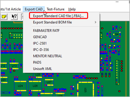
To export the .FBA file, click 'EXPORT CAD'. Then click 'EXPORT STANDARD
CAD FILE [.FBA]' and save the file in the desired directory.

In the box labeled 'CHOOSE FILE' below, click it to browse for the .FBA file
you wish to import. After selecting the file, click 'OPEN'.
Click 'PROCESS FILE' to display the data.
.
If you wish to save the data to a file, click the 'SAVE DATA TO
FILE' button.
The above calculator is provided for informational purposes only.
Unisoft assumes no responsibility for any issues that may arise from its
usage.
Design for Manufacturing/Assembly/Test (DFM/DFA/DFT) for PCB
Manufacturing
Design for Manufacturing, Assembly, and Test
(DFM/DFA/DFT) for PCB manufacturing is a broad and complex subject area.
This comprehensive approach is aimed at designing printed circuit boards
(PCBs) in a manner that facilitates easier and more cost-effective
manufacturing.
DFM/DFA/DFT checks focus on optimizing the PCB design to align with manufacturing capabilities while minimizing potential issues that could arise during production. The primary goals are to enhance production efficiency, reduce costs, and ensure the quality of the final product.
Most aspects of DFM/DFA/DFT are addressed during the PCB design phase, utilizing sophisticated software and techniques provided by various CAD systems. These systems are essential for PCB design, with hundreds of DFM/DFA/DFT criteria to be verified. When applied correctly, adequate DFM/DFA/DFT measures ensure that potential manufacturing, assembly, and testing issues are mitigated before production begins.
Unisoft software, which imports various CAD files and Bills of Materials (BOM) from PCB CAD design systems, assists in verifying that DFM/DFA/DFT principles have been effectively applied to certain aspects of PCB design. For more detailed information on these methods, contact Unisoft directly or refer to the online help tooltips provided.
Areas where
the Unisoft software may assist in verifying that DFM / DFA / DFT was executed properly:
Component Placement
Spacing: The Unisoft software cross-checks that proper spacing between
components is maintained on the PCB by measuring the distance between pins
for unique
reference designators. This spacing is
typically addressed during the design phase of the PCB. Proper component
spacing enables efficient assembly and minimizes issues during soldering
processes.
Test Probe Access
Nets: The Unisoft software verifies that proper test probe access is
available by analyzing each electrical net trace to ensure accessibility for
test probes. This is also typically
addressed during
the PCB design phase. Ensuring adequate test probe access minimizes issues
during the testing phase of manufacturing, including functionality and
quality assurance. This
is a critical Design for Test
(DFT) consideration that facilitates In-Circuit Testing (ICT), Flying Probe
Testing, Functional Testing, and more.
PCB Test Probe Force
Analysis Visualization: Analyzes stresses on the PCB induced by
test probes that press into the PCB, with consideration for offset vectoring
via the placement of push fingers.
Assembly and
Fabrication Notes: Includes detailed notes and specifications for the
manufacturer regarding assembly processes, material requirements, and any
special handling or processing
needs. The Unisoft
software creates process assembly documents to facilitate this.
Supply Chain Considerations:
Design for Manufacturing (DFM), Design for Assembly (DFA), and Design for
Testability (DFT) can extend to include considerations of the supply chain,
such as the
availability of components, lead times,
and the impact of using alternate parts. Early consideration of these
factors helps avoid delays and redesigns caused by unavailable parts or
longer-than-expected
lead times. The Unisoft
software's lookup feature by manufacturer part number, among other
capabilities, can significantly aid in this area.
Webpage proofed using AI in 2024